
 cn.
cn. en.
en.


Explanation: Manufacturability of PCB design
2015-10-13
The manufacturability of PCB design is divided into two categories:
First, it refers to the processing technology of producing printed circuit boards;
Second, it refers to the assembly process of circuit and structural components and printed circuit boards.
For the processing technology of producing printed circuit boards, general PCB manufacturers, due to their manufacturing capacity, will provide designers with relevant requirements in great detail, which is relatively good in practice.
However, according to the author's understanding, what has not been paid enough attention in practice is the second type, namely, design for manufacturability for electronic assembly.
The emphasis of this paper is also to describe the manufacturability issues that must be considered by designers in the PCB design stage.
1. Proper selection of assembly mode and component layout
The selection of assembly mode and component layout is a very important aspect of PCB manufacturability, which has a great impact on assembly efficiency, cost and product quality. In fact, the author has been exposed to quite a number of PCBs, and still lacks some basic principles.
Select the appropriate assembly method
Generally, according to different assembly densities of PCBs, the recommended assembly methods are as follows:
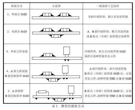
As a circuit design engineer, you should have a correct understanding of the assembly process flow of the designed PCB, so that you can avoid making some principled mistakes. When selecting the assembly mode, in addition to considering the assembly density of PCB and the difficulty of wiring, the typical process flow of this assembly mode must also be taken into account, and the level of process equipment of the enterprise itself.
If our company does not have a good wave soldering process, choosing the fifth assembly method in the table above may cause us great trouble.
In addition, it is worth noting that if the wave soldering process is planned to be implemented on the welding surface, the process complexity caused by a few SMDs arranged on the welding surface should be avoided.
Layout of components
The layout of components on a PCB has a significant impact on production efficiency and cost, and is an important indicator to measure the mountability of PCB design.
In general, components shall be arranged as evenly, regularly and orderly as possible, and arranged in the same direction and polarity.
The regular arrangement is convenient for inspection, is conducive to improving the speed of patch/plug-in, and the uniform distribution is conducive to the optimization of heat dissipation and welding process.
On the other hand, in order to simplify the process flow, PCB designers should always be clear that on either side of a PCB, only one group of soldering processes, including reflow soldering and wave soldering, can be used.
This is especially noteworthy when the assembly density is high and the PCB welding surface must be distributed with more SMD components.
The designer should consider which group welding process to use for the mounting components on the welding surface. The most preferred one is to use the wave soldering process after the curing of the patch, which can weld the pins of the perforated devices on the component surface at the same time; However, the wave soldering patch components have relatively strict constraints, and can only weld chip resistors and capacitors, SOTs, and SOICs of 0603 and above (pin spacing ≥ 1mm and height less than 2.0mm).
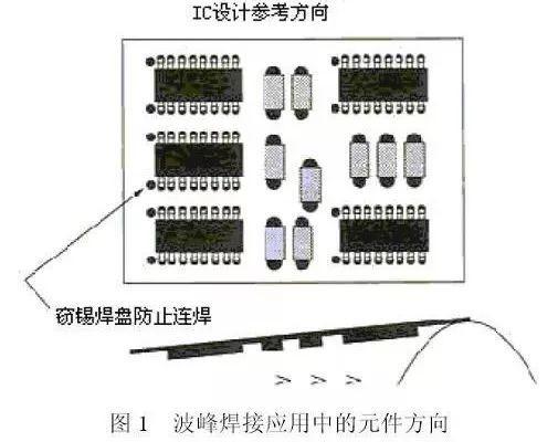
For components distributed on the welding surface, the pin direction should be perpendicular to the transmission direction of the PCB during wave soldering to ensure that the welding ends or leads on both sides of the components are simultaneously submerged, and the arrangement order and spacing between adjacent components should also meet the requirements of wave soldering to avoid "shielding effect", as shown in Figure 1. When wave soldering SOIC and other multi pin components are used, solder pads shall be set at the last two (1 on each side) solder pins in the tin flow direction to prevent continuous soldering.
Components of similar types should be arranged on the board in the same direction, making it easier to mount, inspect and weld components.
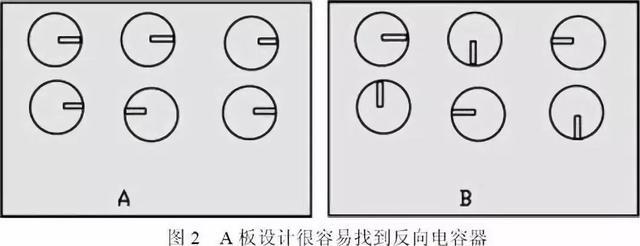
For example, make the negative pole of all radial capacitors face the right side of the board, and make the notch marks of all DIPs face the same direction, which can speed up the insertion and make it easier to find errors.
As shown in Figure 2, since this method is adopted for board A, it is easy to find the reverse capacitor, while it takes more time for board B to find it.
In fact, a company can standardize the direction of all PCB components it manufactures. The layout of some boards may not necessarily allow this, but it should be a direction of effort.
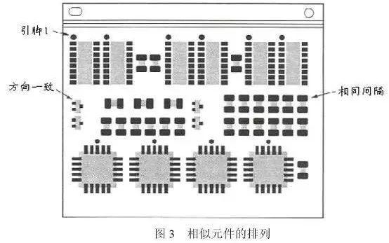
Also, similar element types should be grounded together as much as possible, with the first pin of all elements in the same direction, as shown in Figure 3.
However, the author has indeed met quite a few PCBs with excessive assembly density. High components such as tantalum capacitors and chip inductors must also be distributed on the welding surface of PCBs, and devices such as SOICs and TSOPs with fine spacing. In this case, only double-sided printing solder paste can be used for reflow soldering after mounting, while plug-in components should be concentrated in component distribution as much as possible to adapt to manual welding.
Another possibility is that the perforated elements on the element surface should be distributed on several main straight lines as far as possible to adapt to the latest selective wave soldering process, which can avoid manual welding to improve efficiency and ensure welding quality. Discrete solder joint distribution is a big taboo for selective wave soldering, which will multiply the processing time.
When adjusting the position of components in printed circuit board documents, it must be noted that components and silk screen symbols correspond one by one. If a component is moved without corresponding movement of the silk screen symbol beside the component, it will become a major quality hazard in manufacturing, because in actual production, silk screen symbols are the industry language that can guide production.
2. PCB must be equipped with clamping edges, positioning marks and process positioning holes for automatic production. At present, electronic assembly is one of the industries with the highest degree of automation. All automation equipment used in production requires automatic transmission of PCB, which requires that there is a clamping edge no less than 3-5 mm wide at the top and bottom in the transmission direction of PCB (generally the long side direction) to facilitate automatic transmission, Avoid that components close to the edge of the board cannot be automatically assembled due to clamping.
The function of the positioning mark is that for the assembly equipment widely used for optical positioning at present, the PCB needs to provide at least two to three positioning marks for the optical identification system to accurately position the PCB and correct the processing error of the PCB.
Two of the commonly used positioning marks must be distributed on the diagonal of the PCB. The selection of location marks generally uses standard figures such as solid round pads. To facilitate identification, there should be an open area without other circuit features or marks around the marks. The size should preferably not be less than the diameter of the marks (as shown in Figure 4). The distance between the marks and the board edge should be more than 5 mm.
In the manufacturing of PCB itself, as well as semi-automatic plug-in, ICT testing and other processes in assembly, PCB needs to provide two to three positioning holes at the corners.
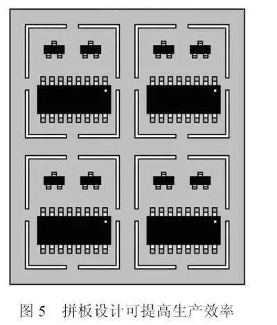
3. Reasonably use panels to improve production efficiency and flexibility
When assembling PCBs with small or irregular dimensions, there are many restrictions. Therefore, the method of splicing boards is generally used to make several small PCBs splice into PCBs of appropriate size for assembly, as shown in Figure 5.
Generally, PCBs with a single side size less than 150mm can be considered to use the splicing method. The size of large PCBs can be spliced to the appropriate processing range through two splicing, three splicing, four splicing, etc. Generally, PCBs with a width of 150mm~250mm and a length of 250mm~350mm are the more appropriate size in automatic assembly.
Another splicing method is to assemble PCBs with SMDs on both sides into a large board, one in front of the other in reverse. This kind of splicing is commonly known as yin-yang splicing, which is generally for the purpose of saving screen board costs. That is, through this kind of splicing, two screen boards were originally required, but now only one screen board needs to be opened.
In addition, when technicians are compiling the operation program of the placement machine, the efficiency of PCB programming using the combination of yin and yang is also higher.
When assembling boards, the connection between sub boards can adopt the methods of double-sided opposite V-shaped groove, long slot hole and round hole, etc., but the design must consider to make the separation line on a straight line as far as possible to facilitate the final board division, and also consider that the separation edge cannot be too close to the PCB line, which may easily damage the PCB during board division.
There is also a very economical panel, which does not mean to panel PCBs, but to panel mesh patterns of screen boards.
With the application of full-automatic solder paste printing machine, the more advanced printing machine has been allowed to operate at a size of 790 × With 790mm steel mesh and multi sided PCB mesh graphics, one piece of steel mesh can be used for printing multiple products, which is a very cost saving practice, especially suitable for manufacturers with small batch and multiple varieties of products.
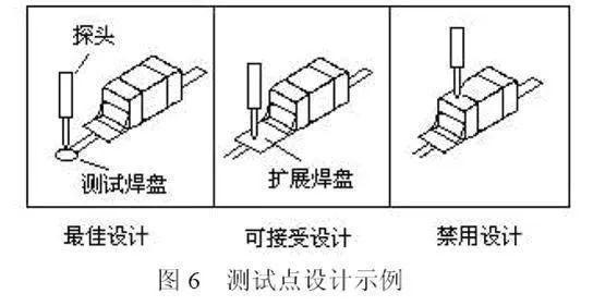
4. Design for Testability Considerations
The testability design of SMT is mainly aimed at the current ICT equipment. The test problems of later product manufacturing are considered in the design of circuit and surface mount printed circuit board (SMB). To improve the testability design, the requirements of process design and electrical design should be considered.
Requirements for process design
The positioning accuracy, substrate manufacturing procedure, substrate size, and probe type are all factors that affect the detection reliability.
Precise locating holes. Set accurate positioning holes on the base plate. The error of positioning holes shall be within ± 0.05mm. At least two positioning holes shall be set, and the farther the distance is, the better. Non metallized locating holes are used to reduce the thickening of the solder coating and fail to meet the tolerance requirements. If the base plate is manufactured as a whole and then tested separately, the positioning hole must be set on the main board and each separate base plate.
The diameter of test points shall not be less than 0.4 mm, and the spacing between adjacent test points shall preferably be more than 2.54 mm and not less than 1.27 mm.
Components with a height of more than * mm shall not be placed on the test surface. Too high components will cause poor contact between the on-line test fixture probe and the test point.
It is better to place the test point 1.0mm away from the components to avoid the impact damage of the probe and components. No components or test points are allowed within 3.2mm around the locating hole ring.
The test point cannot be set within 5mm of the PCB edge. The 5mm space is used to ensure the clamp clamping. Usually, the same process edge is required in the conveyor belt type production equipment and SMT equipment.
It is better to tin all detection points or select metal conductors with soft texture, easy penetration and not easy oxidation to ensure reliable contact and prolong the service life of the probe.
The test point shall not be covered by solder resist or text ink, otherwise the contact area of the test point will be reduced and the reliability of the test will be reduced.
Electrical design requirements
It is required to lead the SMC/SMD test point on the component surface to the welding surface through the via as far as possible, and the via diameter shall be greater than 1mm. In this way, single side needle bed can be used for online testing, thus reducing the cost of online testing.
Each electrical node must have a test point, and each IC must have a power and ground test point as close to this component as possible, preferably within 2.54mm from the IC.
When setting test points on the circuit wiring, the width can be enlarged to 40ml.
Test points shall be evenly distributed on the printed board. If the probe is concentrated in a certain area, the higher pressure will deform the plate to be tested or the needle bed, further causing that some probes cannot contact the test point.
The power supply circuit on the circuit board shall be set with test breakpoints in different areas, so that when the power decoupling capacitor or other components on the circuit board are short circuited to the power supply, the fault point can be found more quickly and accurately. When designing the breakpoint, the power carrying capacity after recovering the test breakpoint shall be considered.
Figure 6 shows an example of a test point design.
Test pads are set near the component leads by extension lines or test nodes are tested by via pads. Test nodes are not allowed to be selected on the solder joints of components. This kind of test may make the faulty solder joints squeezed to the ideal position under the probe pressure, so that the faulty solder joints can be covered, resulting in the so-called "fault shielding effect".
Due to the deflection of the probe caused by positioning error, the probe may directly act on the end point or pin of the component, causing damage to the component.
First, it refers to the processing technology of producing printed circuit boards;
Second, it refers to the assembly process of circuit and structural components and printed circuit boards.
For the processing technology of producing printed circuit boards, general PCB manufacturers, due to their manufacturing capacity, will provide designers with relevant requirements in great detail, which is relatively good in practice.
However, according to the author's understanding, what has not been paid enough attention in practice is the second type, namely, design for manufacturability for electronic assembly.
The emphasis of this paper is also to describe the manufacturability issues that must be considered by designers in the PCB design stage.
1. Proper selection of assembly mode and component layout
The selection of assembly mode and component layout is a very important aspect of PCB manufacturability, which has a great impact on assembly efficiency, cost and product quality. In fact, the author has been exposed to quite a number of PCBs, and still lacks some basic principles.
Select the appropriate assembly method
Generally, according to different assembly densities of PCBs, the recommended assembly methods are as follows:
As a circuit design engineer, you should have a correct understanding of the assembly process flow of the designed PCB, so that you can avoid making some principled mistakes. When selecting the assembly mode, in addition to considering the assembly density of PCB and the difficulty of wiring, the typical process flow of this assembly mode must also be taken into account, and the level of process equipment of the enterprise itself.
If our company does not have a good wave soldering process, choosing the fifth assembly method in the table above may cause us great trouble.
In addition, it is worth noting that if the wave soldering process is planned to be implemented on the welding surface, the process complexity caused by a few SMDs arranged on the welding surface should be avoided.
Layout of components
The layout of components on a PCB has a significant impact on production efficiency and cost, and is an important indicator to measure the mountability of PCB design.
In general, components shall be arranged as evenly, regularly and orderly as possible, and arranged in the same direction and polarity.
The regular arrangement is convenient for inspection, is conducive to improving the speed of patch/plug-in, and the uniform distribution is conducive to the optimization of heat dissipation and welding process.
On the other hand, in order to simplify the process flow, PCB designers should always be clear that on either side of a PCB, only one group of soldering processes, including reflow soldering and wave soldering, can be used.
This is especially noteworthy when the assembly density is high and the PCB welding surface must be distributed with more SMD components.
The designer should consider which group welding process to use for the mounting components on the welding surface. The most preferred one is to use the wave soldering process after the curing of the patch, which can weld the pins of the perforated devices on the component surface at the same time; However, the wave soldering patch components have relatively strict constraints, and can only weld chip resistors and capacitors, SOTs, and SOICs of 0603 and above (pin spacing ≥ 1mm and height less than 2.0mm).
For components distributed on the welding surface, the pin direction should be perpendicular to the transmission direction of the PCB during wave soldering to ensure that the welding ends or leads on both sides of the components are simultaneously submerged, and the arrangement order and spacing between adjacent components should also meet the requirements of wave soldering to avoid "shielding effect", as shown in Figure 1. When wave soldering SOIC and other multi pin components are used, solder pads shall be set at the last two (1 on each side) solder pins in the tin flow direction to prevent continuous soldering.
Components of similar types should be arranged on the board in the same direction, making it easier to mount, inspect and weld components.
For example, make the negative pole of all radial capacitors face the right side of the board, and make the notch marks of all DIPs face the same direction, which can speed up the insertion and make it easier to find errors.
As shown in Figure 2, since this method is adopted for board A, it is easy to find the reverse capacitor, while it takes more time for board B to find it.
In fact, a company can standardize the direction of all PCB components it manufactures. The layout of some boards may not necessarily allow this, but it should be a direction of effort.
Also, similar element types should be grounded together as much as possible, with the first pin of all elements in the same direction, as shown in Figure 3.
However, the author has indeed met quite a few PCBs with excessive assembly density. High components such as tantalum capacitors and chip inductors must also be distributed on the welding surface of PCBs, and devices such as SOICs and TSOPs with fine spacing. In this case, only double-sided printing solder paste can be used for reflow soldering after mounting, while plug-in components should be concentrated in component distribution as much as possible to adapt to manual welding.
Another possibility is that the perforated elements on the element surface should be distributed on several main straight lines as far as possible to adapt to the latest selective wave soldering process, which can avoid manual welding to improve efficiency and ensure welding quality. Discrete solder joint distribution is a big taboo for selective wave soldering, which will multiply the processing time.
When adjusting the position of components in printed circuit board documents, it must be noted that components and silk screen symbols correspond one by one. If a component is moved without corresponding movement of the silk screen symbol beside the component, it will become a major quality hazard in manufacturing, because in actual production, silk screen symbols are the industry language that can guide production.
2. PCB must be equipped with clamping edges, positioning marks and process positioning holes for automatic production. At present, electronic assembly is one of the industries with the highest degree of automation. All automation equipment used in production requires automatic transmission of PCB, which requires that there is a clamping edge no less than 3-5 mm wide at the top and bottom in the transmission direction of PCB (generally the long side direction) to facilitate automatic transmission, Avoid that components close to the edge of the board cannot be automatically assembled due to clamping.
The function of the positioning mark is that for the assembly equipment widely used for optical positioning at present, the PCB needs to provide at least two to three positioning marks for the optical identification system to accurately position the PCB and correct the processing error of the PCB.
Two of the commonly used positioning marks must be distributed on the diagonal of the PCB. The selection of location marks generally uses standard figures such as solid round pads. To facilitate identification, there should be an open area without other circuit features or marks around the marks. The size should preferably not be less than the diameter of the marks (as shown in Figure 4). The distance between the marks and the board edge should be more than 5 mm.
In the manufacturing of PCB itself, as well as semi-automatic plug-in, ICT testing and other processes in assembly, PCB needs to provide two to three positioning holes at the corners.
3. Reasonably use panels to improve production efficiency and flexibility
When assembling PCBs with small or irregular dimensions, there are many restrictions. Therefore, the method of splicing boards is generally used to make several small PCBs splice into PCBs of appropriate size for assembly, as shown in Figure 5.
Generally, PCBs with a single side size less than 150mm can be considered to use the splicing method. The size of large PCBs can be spliced to the appropriate processing range through two splicing, three splicing, four splicing, etc. Generally, PCBs with a width of 150mm~250mm and a length of 250mm~350mm are the more appropriate size in automatic assembly.
Another splicing method is to assemble PCBs with SMDs on both sides into a large board, one in front of the other in reverse. This kind of splicing is commonly known as yin-yang splicing, which is generally for the purpose of saving screen board costs. That is, through this kind of splicing, two screen boards were originally required, but now only one screen board needs to be opened.
In addition, when technicians are compiling the operation program of the placement machine, the efficiency of PCB programming using the combination of yin and yang is also higher.
When assembling boards, the connection between sub boards can adopt the methods of double-sided opposite V-shaped groove, long slot hole and round hole, etc., but the design must consider to make the separation line on a straight line as far as possible to facilitate the final board division, and also consider that the separation edge cannot be too close to the PCB line, which may easily damage the PCB during board division.
There is also a very economical panel, which does not mean to panel PCBs, but to panel mesh patterns of screen boards.
With the application of full-automatic solder paste printing machine, the more advanced printing machine has been allowed to operate at a size of 790 × With 790mm steel mesh and multi sided PCB mesh graphics, one piece of steel mesh can be used for printing multiple products, which is a very cost saving practice, especially suitable for manufacturers with small batch and multiple varieties of products.
4. Design for Testability Considerations
The testability design of SMT is mainly aimed at the current ICT equipment. The test problems of later product manufacturing are considered in the design of circuit and surface mount printed circuit board (SMB). To improve the testability design, the requirements of process design and electrical design should be considered.
Requirements for process design
The positioning accuracy, substrate manufacturing procedure, substrate size, and probe type are all factors that affect the detection reliability.
Precise locating holes. Set accurate positioning holes on the base plate. The error of positioning holes shall be within ± 0.05mm. At least two positioning holes shall be set, and the farther the distance is, the better. Non metallized locating holes are used to reduce the thickening of the solder coating and fail to meet the tolerance requirements. If the base plate is manufactured as a whole and then tested separately, the positioning hole must be set on the main board and each separate base plate.
The diameter of test points shall not be less than 0.4 mm, and the spacing between adjacent test points shall preferably be more than 2.54 mm and not less than 1.27 mm.
Components with a height of more than * mm shall not be placed on the test surface. Too high components will cause poor contact between the on-line test fixture probe and the test point.
It is better to place the test point 1.0mm away from the components to avoid the impact damage of the probe and components. No components or test points are allowed within 3.2mm around the locating hole ring.
The test point cannot be set within 5mm of the PCB edge. The 5mm space is used to ensure the clamp clamping. Usually, the same process edge is required in the conveyor belt type production equipment and SMT equipment.
It is better to tin all detection points or select metal conductors with soft texture, easy penetration and not easy oxidation to ensure reliable contact and prolong the service life of the probe.
The test point shall not be covered by solder resist or text ink, otherwise the contact area of the test point will be reduced and the reliability of the test will be reduced.
Electrical design requirements
It is required to lead the SMC/SMD test point on the component surface to the welding surface through the via as far as possible, and the via diameter shall be greater than 1mm. In this way, single side needle bed can be used for online testing, thus reducing the cost of online testing.
Each electrical node must have a test point, and each IC must have a power and ground test point as close to this component as possible, preferably within 2.54mm from the IC.
When setting test points on the circuit wiring, the width can be enlarged to 40ml.
Test points shall be evenly distributed on the printed board. If the probe is concentrated in a certain area, the higher pressure will deform the plate to be tested or the needle bed, further causing that some probes cannot contact the test point.
The power supply circuit on the circuit board shall be set with test breakpoints in different areas, so that when the power decoupling capacitor or other components on the circuit board are short circuited to the power supply, the fault point can be found more quickly and accurately. When designing the breakpoint, the power carrying capacity after recovering the test breakpoint shall be considered.
Figure 6 shows an example of a test point design.
Test pads are set near the component leads by extension lines or test nodes are tested by via pads. Test nodes are not allowed to be selected on the solder joints of components. This kind of test may make the faulty solder joints squeezed to the ideal position under the probe pressure, so that the faulty solder joints can be covered, resulting in the so-called "fault shielding effect".
Due to the deflection of the probe caused by positioning error, the probe may directly act on the end point or pin of the component, causing damage to the component.


Copyright ©2022 Dongguan Wortech Intelligent Technology Co., Ltd All Rights Reserved ICP888888888