
 cn.
cn. en.
en.


Common problems in PCBA board design and processing
2016-08-10
For most circuit boards, how to set the number of PCBA boards for processing? What factors need to be considered? How to improve the production efficiency and reduce the board loss? Since there are so many advantages of the board assembly, when the PCB design engineer determines the shape of the PCB, he can design the board assembly. Then PCB merging is a problem that needs to be solved in the process of PCBA processing.
Common assembly methods: There are many ways to assemble circuit boards, such as 2-in-1, 3-in-1, 4-in-1, etc. It is common to assemble more than two identical circuit boards into a large circuit board; Different shapes of circuit boards can also be used for splicing, but the application is relatively small, mainly because it is difficult to match the number of boards with different shapes during production; The cathode and anode board is a circuit board composed of the positive and negative sides of the same circuit board. The cathode and anode board can improve the SMT chip processing efficiency and is suitable for circuit boards with fewer components. The design of Yin and Yang boards is not suitable for all circuit boards. If a heavy component is designed in one side of the circuit board, the use of Yin and Yang boards may cause the heavy part to fall off when the side is used as the second printing part. There are also boards with large area of heat absorbing components on the board that cannot be designed with the combination of yin and yang boards. The disadvantage of the male and female plates is that SMT processing is limited, which is easy to cause uneven heating. It is necessary to comprehensively consider all aspects of factors to determine which splicing method to use.
Influence of board making cost on the number of boards
The cost of making boards is the most important factor to measure the number of boards. In order to improve production efficiency and reduce costs, circuit board manufacturers will have basic standard board sizes. These standards repeatedly consider the optimal utilization rate of circuit board boards. Common standards are 16.16 × 16.16”,18.32 × 18.32”,20.32 × 20.32 "etc. The cost of the circuit board will be affected by the size of the board used. Selecting the most appropriate standard board and realizing the optimal utilization of the board can reduce the production cost of the circuit board. The cost of the circuit board is also related to the number of layers and holes of the board, and whether there are blind holes.
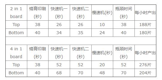
SMT processing line is divided into long line and short line according to different use requirements. The short line has at most two fast mounters and one slow mounter; Long lines usually have multiple fast and slow mounters. Generally, each line is equipped with a tin blue printing machine. It takes about 35-40 seconds to brush the tin for a 150 mm long board assembly. The two in one board is processed in the SMT short line. The newly allocated time for each machine is about 10-26 seconds. The placement time is yuan less than the printing time of the tin stomach, which indicates that the placement machine is waiting for the translation of the printing machine and has not fully utilized the production capacity of the placement machine. Replace two in one with four in one, and the efficiency will be improved immediately (output per hour). See the following table for specific data:
There are many links involved in the manufacturing process of PCBA, so we must control the quality of each link to produce good products. In general, PCBA is a series of processes including PCB manufacturing, component procurement and inspection, SMT chip processing, plug-in processing, program firing, testing, aging, and so on. Let's carefully explain what needs to be paid attention to in each link.
1. After PCB board manufacturing receives the order from PCBA, analyze Gerber documents, pay attention to the relationship between PCB hole spacing and board bearing capacity, do not cause bending or fracture, and whether the wiring takes into account high-frequency signal interference, impedance and other key factors.
2. The purchase of components and parts and the inspection of the purchase of components and parts need to strictly control the channels. We must pick up the goods from large traders and the original factory, and 100% avoid second-hand and fake materials. In addition, special incoming material inspection posts shall be set up to strictly check the following items to ensure that the components are open. Reflow soldering furnace temperature test, no flying wire, whether the vias are blocked or leak ink, whether the board surface is bent, etc; IC checks whether the silk screen is completely consistent with the BOM, and saves it at constant temperature and humidity; Other common materials shall be inspected for screen printing, appearance, power on measurement, etc. The inspection items shall be carried out according to the sampling method, and the proportion is generally 1-3%;
3. SMT assembly, solder paste printing and reflow soldering furnace temperature control are key points, and it is very important to use laser steel mesh with good quality and meeting process requirements. According to the requirements of PCB, some of the steel mesh holes need to be increased or reduced, or U-shaped holes are used. The steel mesh is made according to the process requirements. The furnace temperature and speed of reflow soldering control the immersion of solder paste
4. The reliability of lubrication and welding is very critical, and it can be controlled according to the normal SOP operation guidelines. In addition, AOI detection should be strictly carried out to minimize the defects caused by human factors.
5. In DIP plug-in processing and plug-in process, mold design for wave soldering is the key point. How to use the mold to maximize the probability of good products after the furnace is a process that PE engineers must constantly practice and summarize experience. In the previous DFM report, the program control can advise customers to set some test points on the PCB. The purpose is to test the continuity of PCB and PCBA circuit after all components are welded. If conditions permit, the customer can be asked to provide a program to burn the program into the main control IC through a burner (such as ST-LINK, J-LINK, etc.), so that the functional changes caused by various touch actions can be tested more intuitively, so as to check the functional integrity of the entire PCBA. PCBA board test For orders with PCBA test requirements, the main test contents include LCT (In Cicuit Test), FCT (Function Test), Burn In Test (Aging Test), temperature and humidity test, drop test, etc. The specific operation is based on the customer's test plan and the report data can be summarized.
Common assembly methods: There are many ways to assemble circuit boards, such as 2-in-1, 3-in-1, 4-in-1, etc. It is common to assemble more than two identical circuit boards into a large circuit board; Different shapes of circuit boards can also be used for splicing, but the application is relatively small, mainly because it is difficult to match the number of boards with different shapes during production; The cathode and anode board is a circuit board composed of the positive and negative sides of the same circuit board. The cathode and anode board can improve the SMT chip processing efficiency and is suitable for circuit boards with fewer components. The design of Yin and Yang boards is not suitable for all circuit boards. If a heavy component is designed in one side of the circuit board, the use of Yin and Yang boards may cause the heavy part to fall off when the side is used as the second printing part. There are also boards with large area of heat absorbing components on the board that cannot be designed with the combination of yin and yang boards. The disadvantage of the male and female plates is that SMT processing is limited, which is easy to cause uneven heating. It is necessary to comprehensively consider all aspects of factors to determine which splicing method to use.
Influence of board making cost on the number of boards
The cost of making boards is the most important factor to measure the number of boards. In order to improve production efficiency and reduce costs, circuit board manufacturers will have basic standard board sizes. These standards repeatedly consider the optimal utilization rate of circuit board boards. Common standards are 16.16 × 16.16”,18.32 × 18.32”,20.32 × 20.32 "etc. The cost of the circuit board will be affected by the size of the board used. Selecting the most appropriate standard board and realizing the optimal utilization of the board can reduce the production cost of the circuit board. The cost of the circuit board is also related to the number of layers and holes of the board, and whether there are blind holes.
SMT processing line is divided into long line and short line according to different use requirements. The short line has at most two fast mounters and one slow mounter; Long lines usually have multiple fast and slow mounters. Generally, each line is equipped with a tin blue printing machine. It takes about 35-40 seconds to brush the tin for a 150 mm long board assembly. The two in one board is processed in the SMT short line. The newly allocated time for each machine is about 10-26 seconds. The placement time is yuan less than the printing time of the tin stomach, which indicates that the placement machine is waiting for the translation of the printing machine and has not fully utilized the production capacity of the placement machine. Replace two in one with four in one, and the efficiency will be improved immediately (output per hour). See the following table for specific data:
There are many links involved in the manufacturing process of PCBA, so we must control the quality of each link to produce good products. In general, PCBA is a series of processes including PCB manufacturing, component procurement and inspection, SMT chip processing, plug-in processing, program firing, testing, aging, and so on. Let's carefully explain what needs to be paid attention to in each link.
1. After PCB board manufacturing receives the order from PCBA, analyze Gerber documents, pay attention to the relationship between PCB hole spacing and board bearing capacity, do not cause bending or fracture, and whether the wiring takes into account high-frequency signal interference, impedance and other key factors.
2. The purchase of components and parts and the inspection of the purchase of components and parts need to strictly control the channels. We must pick up the goods from large traders and the original factory, and 100% avoid second-hand and fake materials. In addition, special incoming material inspection posts shall be set up to strictly check the following items to ensure that the components are open. Reflow soldering furnace temperature test, no flying wire, whether the vias are blocked or leak ink, whether the board surface is bent, etc; IC checks whether the silk screen is completely consistent with the BOM, and saves it at constant temperature and humidity; Other common materials shall be inspected for screen printing, appearance, power on measurement, etc. The inspection items shall be carried out according to the sampling method, and the proportion is generally 1-3%;
3. SMT assembly, solder paste printing and reflow soldering furnace temperature control are key points, and it is very important to use laser steel mesh with good quality and meeting process requirements. According to the requirements of PCB, some of the steel mesh holes need to be increased or reduced, or U-shaped holes are used. The steel mesh is made according to the process requirements. The furnace temperature and speed of reflow soldering control the immersion of solder paste
4. The reliability of lubrication and welding is very critical, and it can be controlled according to the normal SOP operation guidelines. In addition, AOI detection should be strictly carried out to minimize the defects caused by human factors.
5. In DIP plug-in processing and plug-in process, mold design for wave soldering is the key point. How to use the mold to maximize the probability of good products after the furnace is a process that PE engineers must constantly practice and summarize experience. In the previous DFM report, the program control can advise customers to set some test points on the PCB. The purpose is to test the continuity of PCB and PCBA circuit after all components are welded. If conditions permit, the customer can be asked to provide a program to burn the program into the main control IC through a burner (such as ST-LINK, J-LINK, etc.), so that the functional changes caused by various touch actions can be tested more intuitively, so as to check the functional integrity of the entire PCBA. PCBA board test For orders with PCBA test requirements, the main test contents include LCT (In Cicuit Test), FCT (Function Test), Burn In Test (Aging Test), temperature and humidity test, drop test, etc. The specific operation is based on the customer's test plan and the report data can be summarized.


Copyright ©2022 Dongguan Wortech Intelligent Technology Co., Ltd All Rights Reserved ICP888888888